As semiconductor manufacturing advances to finer process nodes, wafer-level defect analysis, failure location, and micro-nano fabrication have become key to improving yield. CIQTEK introduces the 8-inch Wafer Dual-Beam Full-Size Processing Solution, combining high-resolution imaging and precise ion beam processing to achieve "observation-analysis-cutting" across the entire wafer, providing strong technical support for advanced semiconductor processes.
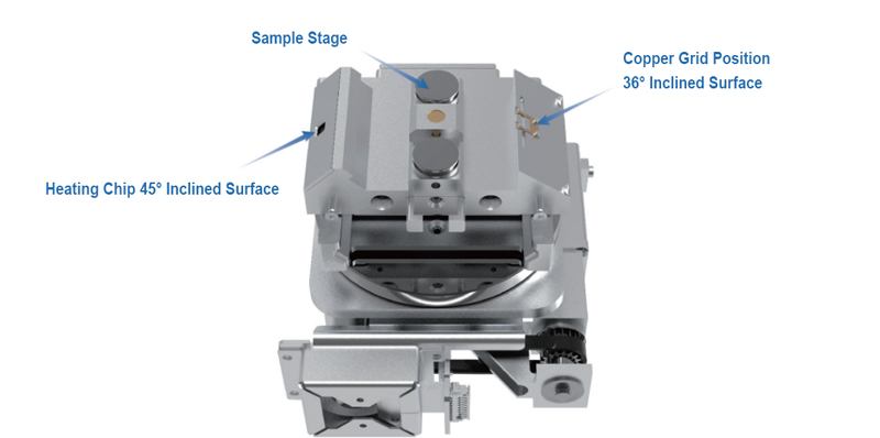
This solution features a 150mm long-stroke high-precision sample stage, enabling full-wafer, non-destructive observation and processing of 8-inch wafers. With an external optical navigation system and intelligent anti-collision algorithms, it ensures rapid and precise wafer positioning and safe operation. The system is equipped with a Schottky field emission electron gun, offering a resolution of 0.9 nm @ 15kV, and an ion beam resolution of 3 nm @ 30kV, capable of defect detection, cross-section slicing, and micro-structure fabrication at the nanoscale.
Core Advantages:
- 150mm Travel Stage:
-
-
Combines long travel with high precision for an extensive observation range.
-
Excellent compatibility with different-sized fixtures.
-
Robust structure ensures wafer stability and quick, reliable loading.
-
- 8-inch Quick Exchange:
-
Intelligent weight-bearing design with a sliding base for stability and durability.
-
Full-size compatibility: Supports 2/4/6/8-inch wafers.
-
Fast sample exchange: Vacuum pumping and sample loading within one minute.
-
- Software and Anti-Collision:
-
-
Fully automatic intelligent navigation with accurate movement and positioning.
-
Multi-axis coordinated motion for full-wafer observation.
-
Smart anti-collision: Trajectory simulation and algorithmic spatial calculations to avoid risks.
-
Multiple real-time monitoring: Real-time multi-angle monitoring of wafer position.
-
-
External Optical Navigation:
-
Ultra-stable structure design suppresses image shake.
-
High-definition imaging with a precise field of view for full-wafer display.
-
Professional anti-glare lighting reduces wafer surface reflection.
-
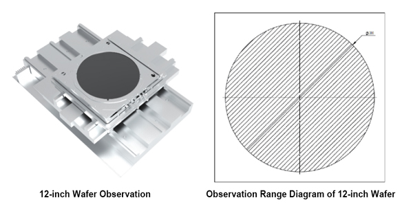
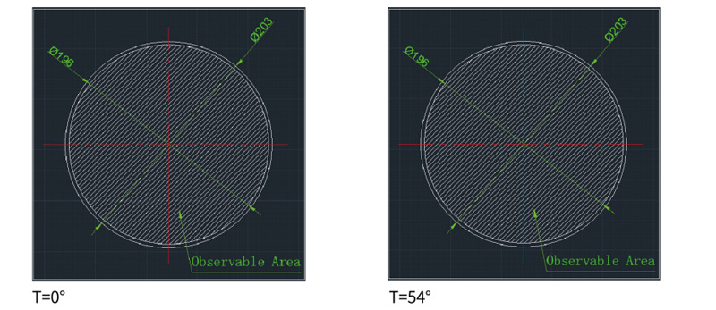
Wafer observation range
CIQTEK Dual-Beam Electron Microscope Solution combines outstanding hardware with intelligent software systems, enabling efficient defect detection and process optimization through one-click brightness and contrast adjustment, auto-focus, and multi-format image output, empowering users to complete the full chain of tasks from defect discovery to process optimization.