First. Why End-Face Quality is Critical
In fiber laser systems, optical connectors act as gateways for high-intensity light. An ideal end-face is perfectly clean, smooth, and free of defects. However, in an industrial environment, end-faces are susceptible to:
· Contamination: Dust, oil, fingerprints, and moisture.
·Damage: Scratches, pits, and cracks (chipping).
Even microscopic contaminants can absorb laser energy, leading to thermal lensing, power loss, and, ultimately, irreversible damage to the coating or the fiber itself. A damaged end-face can scatter light, reduce beam quality, and cause a dangerous back-reflection that can destroy the pump sources or gain modules.
Second. The Golden Rule: Inspect Before Every Connection
The single most important practice in fiber laser maintenance is to inspect the fiber end-face both before disconnecting and after cleaning, prior to reconnection. A visual inspection takes only moments but can prevent costly downtime and component replacement.
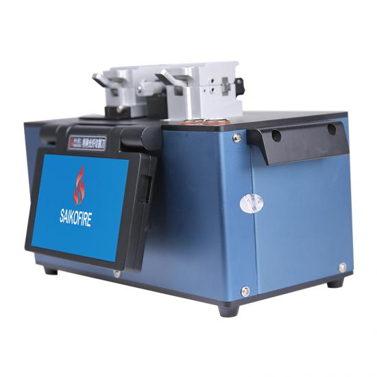
Third. Inspection Tools: The Fiber Microscope
The primary tool for end-face inspection is a specialized fiber inspection microscope.
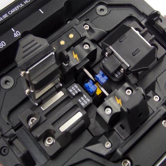
· Types: Handheld probes, benchtop stations, and video microscopes.
·Magnification: Typically 200x to 400x. For single-mode fibers and high-power applications, 400x magnification is the industry standard for detailed analysis.
·Interfaces: Probes come with various adapters (e.g., FC/APC, SC) to fit different connector types. It is crucial to use the correct adapter to avoid damaging the probe or the connector.
Inspection Process:
1. Ensure the laser is powered down and all safety protocols are followed.
2. Select the correct microscope adapter for the connector.
3. Gently insert the connector into the microscope.
4. Capture a clear image and analyze it systematically.
Fourth. Interpreting the Inspection: Acceptance vs. Rejection
Analyze the end-face by dividing it into zones, with the core being the most critical area.
a) Pass / Acceptable:
·The end-face is clean, with no visible contamination.
·The core, cladding, and connector surface are flawless under magnification.
·Action: Safe to connect.
b) Contaminated - Requires Cleaning:
·Presence of dust, oil, water stains, or other particulates.
·Action: Proceed with cleaning using the appropriate method .
c) Fail / Reject - Requires Re-termination or Replacement:
·Scratches: Deep scratches running through the core region.
·Cracks/Chipping: Damage to the edge of the ferrule, especially if propagating inward.
·Pits & Bulk Damage: Evidence of melting, burning, or ablation at the core. This is often a "catastrophic defect" caused by operating the laser with a contaminated end-face. This defect will only worsen with use.
·Fixed Contamination: Contaminants that are bonded or burned onto the surface and cannot be removed by cleaning.
·Action: DO NOT CONNECT. The fiber must be re-terminated (re-cleaved and re-polished) or the patch cord/component must be replaced.
Fifth. Cleaning Procedures: The One-Way Wipe
The goal of cleaning is to remove contaminants without introducing new scratches or static charge.
Method 1:
Dry Cleaning (For loose, dry particles)
·Tool: Fiber optic cleaning pen (Cletop-type) or one-click cleaner.
·Procedure:
1. Open the cleaner to reveal a fresh lint-free tape or pad.
2. Bring the connector ferrule down onto the tape at a slight angle.
3. Wipe in a single, straight motion. Do not rub back and forth.
4. Close the cleaner to protect the tape.
5. Immediately re-inspect the end-face.
Method 2: Wet-to-Dry Cleaning (For stubborn contaminants, oils)
·Tools: Lint-free wipes and spectroscopic-grade isopropyl alcohol (IPA, >=99%).
·Procedure:
1. Apply a small drop of IPA to a fresh, clean area of a lint-free wipe.
2. Gently wipe the end-face once across the wet area.
3. Immediately wipe the end-face once across a dry area of a fresh wipe to remove any residue and dry the surface.
4. Immediately re-inspect the end-face.
Important Notes on Cleaning:
·Never use compressed air from an industrial line, as it contains oil and moisture and can blast contaminants into the end-face.
·Use solvents specifically designed for fiber optics. Lower-grade IPA can leave residues.
·Always use a fresh part of a wipe or a new cleaning tape for each cleaning attempt.
Sixth. Best Practices and Prevention
·Always Use Protective Caps: Install dust caps on all connectors and bulkhead ports when not in use.
·Avoid Contact: Never touch the end-face of a ferrule. Handle connectors by the body.
·Control the Environment: Perform connections in as clean an environment as possible.
·Proper Torque: Use a torque wrench for threaded connectors (like FC) to avoid over-tightening, which can cause physical stress and misalignment.
For high-power fiber laser systems, there is no room for compromise on fiber optic connector care. Implementing a rigorous culture of "inspect, clean, and re-inspect" is not merely a best practice—it is a fundamental requirement for ensuring system reliability, maximizing uptime, and protecting significant capital investment. A clean fiber is a reliable fiber.
Fiber Optic End-Face FAQs
Q1: Why is it so critical to inspect and clean a fiber optic end-face in a laser system?
A:In high-power laser systems, the laser beam is focused onto a tiny core of the fiber. Any contamination (dust, oil) or damage (scratches, pits) on the end-face can absorb laser energy, generating intense heat. This leads to:
·Power Loss: Reduced laser output.
·Beam Quality Degradation: Poor focusability, leading to bad processing results.
·Catastrophic Failure: The contaminated or damaged spot can burn, causing permanent damage to the fiber and potentially back-reflecting light to destroy other expensive components like pump diodes.
Q2: What is the single most important rule when working with fiber connections?
A:The golden rule is: "Inspect Before Every Connection." You should inspect the end-face both before you disconnect it (to establish a baseline) and after you clean it, before you reconnect it. This simple habit is the most effective way to prevent most fiber-related failures.
Q3: What is the difference between a end-face that just needs cleaning versus one that needs to be replaced?
A:
·Needs Cleaning: The end-face has contaminants like dust, oil, or fingerprints that are on top of the surface. These can be removed.
·Needs Replacement: The end-face has permanent physical damage. Key signs include:
·Deep scratches running through the core.
·Cracks or chipping at the edge of the ferrule.
·Pits or burn marks (catastrophic defects), especially in the core, which look like melted or ablated spots.