Italy has long been a hub for innovation in materials science, nanotechnology, and cultural heritage preservation. Across the country’s universities and national research centers, scanning electron microscopy (SEM) plays a central role in analyzing microstructures and surface morphologies with high precision. In 2025, the demand for advanced SEM systems in Italy continues to rise, driven by the pursuit of higher resolution, improved automation, and multi-mode analytical capabilities.
SEM as a Core Tool in Italian Research
From the Politecnico di Milano to the National Research Council (CNR) and major materials institutes in Emilia-Romagna, SEM has become indispensable for both academic and industrial research. Italian laboratories rely on these systems to study metals, ceramics, semiconductors, biological samples, and even ancient artifacts.
Recent years have seen a shift from conventional tungsten SEMs to field emission SEM (FE-SEM) platforms, which deliver higher spatial resolution and more stable imaging performance. This evolution reflects the country’s growing focus on nanostructured materials, energy devices, and precision manufacturing — all areas where nanoscale imaging and analysis are crucial.
Performance Priorities for Italian SEM Users
Italian researchers tend to emphasize several practical factors when evaluating SEM systems:
-
Resolution and imaging stability: The ability to observe nanoscale details in materials such as thin films, catalysts, and nanocomposites.
-
Analytical integration: Compatibility with EDS, EBSD, and WDS systems to extract chemical and crystallographic information alongside morphology.
-
Ease of operation and automation: Software-guided imaging and recipe-based workflows are increasingly preferred in multi-user facilities.
-
Temperature and environmental control: In-situ observation of microstructural evolution under heating or vacuum changes is becoming more common.
-
Service and long-term support: Access to local technical expertise and responsive maintenance is a key factor in supplier selection.
These priorities reflect a broader trend: Italian laboratories are modernizing not only their instrumentation but also their workflow efficiency and data reliability.
Modern SEM Systems Entering the Italian Market
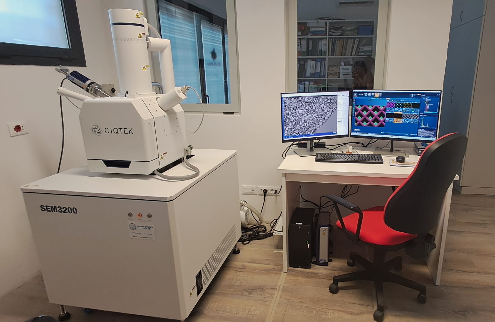
In recent years, CIQTEK’s SEM instruments have been increasingly adopted by research and industrial users across Italy. Several systems, including the SEM3200 and SEM3300, have been installed through CIQTEK’s local partner in Rome. It has also established a dedicated CIQTEK SEM demonstration laboratory, where Italian researchers can experience the imaging performance and analytical capabilities of the systems firsthand. These installations highlight the country’s growing interest in high-resolution, stable, and user-friendly SEMs supported by local expertise.
A Growing Ecosystem for Advanced Electron Microscopy
Italy’s strong tradition in materials and applied sciences continues to drive demand for advanced electron microscopy. National research centers, universities, and technology companies are jointly shaping a dynamic environment where innovation in imaging and analysis thrives.
With more international suppliers now offering localized support and demonstration facilities, such as CIQTEK’s growing presence through its partner network, Italian users have access to an expanding ecosystem of high-performance, reliable SEM solutions. In addition to advanced imaging quality and stable performance, CIQTEK SEM systems are recognized for their competitive pricing, making high-end field emission microscopy more accessible to a wider range of research and industrial users.
This growing accessibility, combined with strong local technical support, ensures that Italy remains at the forefront of microscopy research and application in Europe, where precision, performance, and affordability converge to empower the next generation of scientific discovery.
