Affordable SEM for Resource-Limited Environments What to Look For

For many universities, national labs, and research institutes in regions such as Africa and the Middle East, access to advanced scientific instrumentation is often limited by budget, infrastructure, and maintenance challenges. Scanning Electron Microscopes (SEMs) are essential tools for materials science, life sciences, and education, but traditional models can be prohibitively expensive and difficult to maintain.

This is why affordable SEM solutions have become critical for resource-limited environments. But "affordable" should not mean compromising on performance or usability. Below, we explore the key factors to consider when selecting a cost-effective SEM and how CIQTEK is helping research communities worldwide overcome these challenges.


Why Resource-Limited Labs Need Affordable SEMs

In developing regions, researchers often face unique barriers:

  • Budget Constraints – High upfront costs and ongoing maintenance make many SEMs inaccessible. 

  • Infrastructure Limitations – Power supply stability, room conditions, and service availability can restrict choices.

  • Educational Demands – Universities need SEMs that are easy to learn, operate, and maintain for student training.

  • Service and Support Gaps – Remote locations often lack local technical support, making reliability and remote assistance crucial.

For example, a university in East Africa wanted to give engineering students access to SEM imaging. A million-dollar instrument was out of reach, but a cost-effective, compact SEM made it possible to expand their curriculum and attract new research collaborations; A national lab in the Middle East struggled with power fluctuations that frequently disrupted their older high-end SEM. Switching to a robust, lower-maintenance system ensured consistent imaging and reduced downtime.


What to Look for in an Affordable SEM

When evaluating SEM options for resource-limited labs, consider the following:

  • Total Cost of Ownership
    Not just the purchase price, factor in maintenance, consumables, and energy use.

  • Ease of Use
    A user-friendly interface helps reduce training costs and allows students and new researchers to get hands-on quickly.

  • Durability & Reliability
    Instruments should perform consistently even in less-than-ideal lab conditions.

  • Remote Support & Training
    For institutions far from service centers, remote diagnostics, online training, and virtual demonstrations are essential.

  • Scalability
    SEMs should be versatile enough to support both teaching and research, making them a long-term investment.


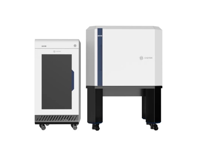
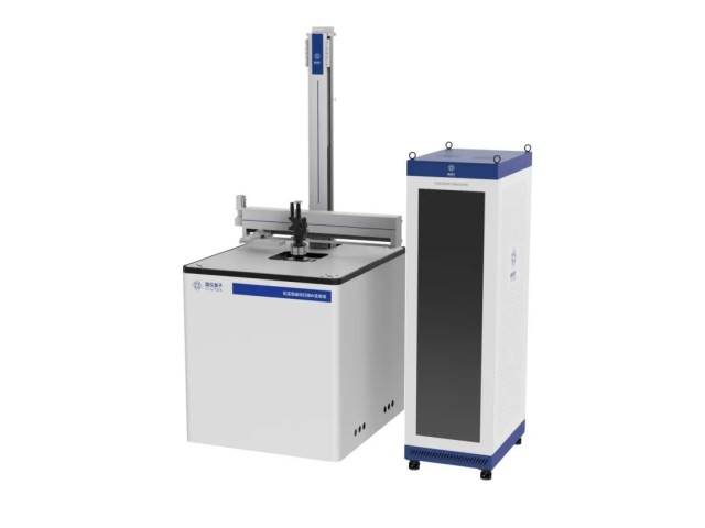
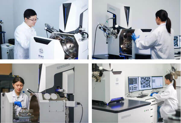
CIQTEK SEM: Affordable Without Compromise

At CIQTEK, we’ve worked with institutions worldwide to deliver SEMs that combine affordability with reliability. Our systems are designed for teaching labs, national facilities, and emerging research groups that need dependable performance without excessive cost.

  • Budget-Friendly Pricing – Enables universities and labs to invest in advanced imaging while leaving room for consumables, training, or lab expansions.

  • Low Maintenance Design – Reduced service needs mean fewer interruptions and lower long-term costs.

  • User-Friendly Interface – Ideal for classrooms, making SEM operation accessible to undergraduates and postgraduates alike.

  • High-Quality Imaging – Clear results suitable for materials science, biology, and applied engineering research.


Whether for a teaching university in Africa or a national lab in the Middle East, CIQTEK SEMs provide a reliable and affordable choice that empowers scientific discovery.

CIQTEK SEM microscope


>> If you’re looking for a cost-effective SEM, contact CIQTEK today to learn how our SEM instruments can support your research and teaching needs.

Continue
\"Nature Materials\"- CIQTEK SNVM Assists Customers in Achieving Key Breakthroughs in Graphene Spin Devices

Recently, a team led by Wang Haomin from the Shanghai Institute of Microsystem and Information Technology of the Chinese Academy of Sciences made significant progress in studying the magnetism of zigzag graphene nanoribbons (zGNRs) using a CIQTEK Scanning Nitrogen-vacancy Microscope (SNVM).


Building on previous research, the team pre-etched hexagonal boron nitride (hBN) with metal particles to create oriented atomic trenches and used a vapor-phase catalytic chemical vapor deposition (CVD) method to controllably prepare chiral graphene nanoribbons in the trenches, obtaining ~9 nm wide zGNRs samples embedded in the hBN lattice. By combining SNVM and magnetic transport measurements, the team directly confirmed its intrinsic magnetism in experiments. This groundbreaking discovery lays a solid foundation for the development of graphene-based spin electronic devices. The related research findings, titled "Signatures of magnetism in zigzag graphene nanoribbons embedded in a hexagonal boron nitride lattice," have been published in the prestigious academic journal "Nature Materials".


Graphene, as a unique two-dimensional material, exhibits magnetic properties of p-orbital electrons that are fundamentally different from the localized magnetic properties of d/f orbital electrons in traditional magnetic materials, opening up new research directions for exploring pure carbon-based magnetism. Zigzag graphene nanoribbons (zGNRs), potentially possessing unique magnetic electronic states near the Fermi level, are believed to hold great potential in the field of spin electronics devices. However, detecting the magnetism of zGNRs through electrical transport methods faces multiple challenges. For instance, nanoribbons assembled from the bottom up are often too short in length to reliably fabricate devices. Additionally, the high chemical reactivity of zGNR edges can lead to instability or uneven doping. Furthermore, in narrower zGNRs, the strong antiferromagnetic coupling of edge states can make it difficult to detect their magnetic signals electrically. These factors hinder direct detection of the magnetism in zGNRs.


ZGNRs embedded in the hBN lattice exhibit higher edge stability and feature an inherent electric field, creating ideal conditions for detecting the magnetism of zGNRs. In the study, the team used CIQTEK's Room-Temperature SNVM to observe the magnetic signals of zGNRs directly at room temperature.


Figure 1: Magnetic measurement of zGNR embedded in a hexagonal boron nitride lattice using Scanning Nitrogen-vacancy Microscope


In electrical transport measurements, the fabricated approximately 9-nanometer-wide zGNR transistors demonstrated high conductivity and ballistic transport characteristics. Under the influence of a magnetic field, the device exhibited significant anisotropic magnetoresistance, with a magnetoresistance change of approximately 175 Ω at 4 K, a magnetoresistance ratio of about 1.3%, and this signal persisted even at temperatures as high as 350 K. Hysteresis was only observed under a magnetic field perpendicular to the plane of the zGNRs, confirming its magnetic anisotropy. Through analysis of the variation of magnetoresistance with tilting angle, the researchers found that the magnetic moment is perpendicular to the sample surface. Furthermore, the decrease in magnetoresistance with increasing source-drain bias and temperature revealed the interaction between magnetic response and charge transport and thermal vibrations.


Figure 2: Magnetic transport characteristics of 9-nanometer-wide zGNR devices embedded in hBN


This research, by combining Scanning Nitrogen-vacancy Microscope technology and transport measurements, directly confirmed the existence of intrinsic magnetism in hBN-embedded zGNRs for the first time, providing a possibility for controlling magnetism through an electric field. This work not only deepens the understanding of graphene's magnetic properties but also opens up new pathways for the development of spin electronic devices based on graphene.


Experience the Nano-scale Magnetic Imaging System


CIQTEK invites you to experience the Scanning Nitrogen-vacancy Microscope (SNVM) – a globally leading nano-scale magnetic field imaging system, operating at temperatures of 1.8~300 K with a vector magnetic field of 9/1/1 T, achieving a magnetic spatial resolution of 10 nm, and magnetic sensitivity of 2 μT/Hz1/2.


SNVM is a precision measurement instrument that combines Diamond Nitrogen-vacancy (NV) Optically Detected Magnetic Resonance (ODMR) technology with Atomic Force Microscopy (AFM) scanning imaging technology. It features high spatial resolution, high-sensitivity magnetic imaging, versatile detection capabilities, and non-invasive detection advantages, making it important in areas such as magnetic domain characterization, antiferromagnetic imaging, superconductor characterization, and research on two-dimensional magnetic materials.

Room temperature version of SNVM

Cryogenic version of SNVM


Continue
Beyong Nano Showcases CIQTEK SEM3200 at the 33rd International Materials Research Congress 2025 in Mexico

Beyong Nano, a leading innovator in nanotechnology, is set to unveil its groundbreaking model CIQTEK SEM3200 at the prestigious 33rd International Materials Research Congress taking place in Cancun, Mexico.


The Congress, known for bringing together pioneers and visionaries in the field of materials science, provides Beyong Nano with the perfect platform to showcase CIQTEKlatest technological marvel.


The Scanning Electron Microscope is poised to revolutionize the industry with its advanced features, unparalleled performance, and potential applications across various sectors. 


Visitors to the Beyong Nano booth at the congress can experience firsthand the transformative potential of the model 3200 and engage with the company's team of experts to learn more about its features, applications, and future developments.

Continue
CIQTEK at The Egyptian Society of Electron Microscopy Conference 2025

We, CIQTEK, are pleased to invite you to the Electron Microscopy Conference 2025, held from October 13th to 15th, 2025, at the Theodor Bilharz Research Institute, Egypt. 


The theme of this year's conference is: "The Importance of Electron Microscopy in Enlightening the Invisible". It reflects the profound impact that electron microscopy continues to have across diverse scientific disciplines, from biology to materials science.


Over the conference's three days, we will have the opportunity to engage in in-depth tutorials, keynote sessions, and explore the latest technological advancements in the field of Electron MicroscopesIt will follow a Hybrid format, allowing participants from around the world to join us both in person and virtually, ensuring an inclusive and accessible experience for all.


Meet us at ESEM

Date: October 13 - 15, 2025


LocationTheodor Bilharz Research Institute, Egypt


Continue
Understanding Quartz Crystal Frequency Characteristics Selecting the Optimal Oscillator Solution for Your Needs

The basic working principle of quartz crystal oscillator

Quartz crystal oscillators utilize high-quality piezoelectric crystals, harnessing the piezoelectric effect to generate stable oscillations. The crystal's quality factor (Q) directly impacts frequency stability—a higher Q provides a more accurate and reliable clock signal. The vibration frequency characteristics are determined by three key factors: crystal thickness, crystal geometry, and cutting method.


Effect of thickness on frequency

The frequency of a quartz crystal is inversely proportional to the thickness of the crystal:

Thin wafers: Support higher oscillation frequencies, ideal for high-frequency applications.

Thick wafers: small vibration amplitude and excellent resistance to mechanical shock

Technological breakthrough : Overtone crystal technology enables a chip with a fundamental frequency of 20MHz to reach 100MHz through the fifth overtone, allowing medium and low fundamental frequency chips to meet high-frequency requirements of hundreds of megahertz.


Chip shape and frequency characteristics


Tuning Fork Chip

Typical application: 32.768kHz crystal oscillator

Typical dimensions: 3.2 × 1.5 × 0.8 mm

Temperature characteristics: parabolic characteristics of -0.04ppm/℃²

Manufacturing process: Photolithography technology is used to achieve micron-level precision

Frequency determining factors: mainly depends on the fork length (L), the longer the length, the higher the frequency

Advantages: Especially suitable for low-frequency precise timing scenarios


Fectangular Wafer

Frequency range: MHz level application

Miniaturization: From 7.0×5.0mm to 1.6×1.2mm

High frequency: Up to 300MHz through chamfered edge technology

Low power consumption: current consumption can be as low as 0.5μA

Main features: convenient for large-scale production and standardized packaging

Frequency Determinants: Thickness is the Main Influencing Factor


Comparison of key cutting technologies

The cutting angle of the quartz crystal (defined in the XYZ coordinate system) directly affects:

(1) Long-term aging characteristics

(2) Temperature stability

(3) Frequency accuracy

Mainstream cutting methods : AT cutting, BT cutting, SC cutting, IT cutting, and special cutting processes designed specifically for tuning fork wafers. Each method has its own performance advantages and applicable scenarios.


Contact

Need the optimal quartz crystal oscillator solution for your application? Our team of engineers can provide complete crystal oscillator selection recommendations and technical support, from low to high frequencies, based on your specific application needs.

Please contact our sales team:  

Tel: 0086-576-89808609  

Email: market@acrystals.com

Website: [www.acrystals.com](http://www.acrystals.com)  

Continue
The HK72 - Your Slim, Smart Health Companion

Finding a comfortable yet capable health tracker just got easier with the HK72 smart bracelet. This ultra-light 38g wearable disappears on your wrist with its barely-there 9.9mm metal body, proving you don't need bulk for advanced features. The vibrant 1.47-inch AMOLED screen delivers crisp notifications and health data at a glance, while the 10-day battery life outlasts most smartwatches.


What sets the HK72 apart is its thoughtful health tracking. It automatically monitors your heart rate and blood oxygen around the clock, with special attention to women's health through menstrual cycle tracking. The sleep analysis breaks down your REM cycles, while the stress monitor suggests breathing exercises when tension rises. Unlike complex smartwatches, it presents this data simply through an intuitive interface.


For active users, the IP68 waterproof rating means no workout is off-limits - whether swimming laps or running in rain. The bracelet automatically detects exercise types and tracks progress through three motivational activity rings. Smart features like Bluetooth calling and offline Alipay payments add convenience without complicating the experience. With multiple stylish watch faces and an always-on display option, the HK72 blends seamlessly into both gym sessions and business meetings - a rare balance of form and function in wearable tech.

Ultra thin AMOLED smart braceletOEM smart bracelet supplierCustom logo fitness trackers

Continue
CIQTEK to Showcase Advanced Scientific and Oilfield Instruments at ARABLAB 2025 in Dubai

CIQTEK is excited to announce our participation in ARABLAB 2025, one of the leading international trade shows for laboratory technology, scientific instruments, and petroleum exploration equipment. The event will take place from 23 to 25 September 2025 at the Dubai World Trade Center, UAE, and visitors can find us at Booth H1-C24, Sheikh Saeed Hall 1.


At the exhibition, CIQTEK will present our latest innovations in electron microscopy (FIB/SEM, TEM), electron paramagnetic resonance (EPR) spectrometers, BET Surface Area &Porosimetry Analyzers, and other advanced analytical instruments. The team will demonstrate product capabilities, share real-world application success stories, and discuss solutions for researchers and industrial professionals across multiple sectors.


In addition, CIQTEK will introduce QOILTECH, our specialized brand for innovating petroleum exploration and oilfield services. QOILTECH focuses on the R&D, manufacturing, and sales of petroleum exploration equipment, including RSS, MWD/LWD, resistivity, and near-bit azimuth gamma tools, designed for extreme environments. With proven expertise in tool design and application, QOILTECH delivers equipment capable of operating at depths of up to 100,000 meters annually, supporting efficient and reliable petroleum logging while drilling operations.


QOILTECH oilfield services


ARABLAB provides a key platform to connect with industry experts, researchers, and distributors from around the world. CIQTEK looks forward to engaging with attendees, showcasing how our advanced scientific instruments and petroleum exploration tools can drive breakthroughs in research, industrial applications, and oilfield operations.

We warmly invite you to visit our booth at H1-C24 to experience our instruments in action and speak directly with our product specialists.

Event Details:


  • Date: 23–25 September 2025

  • Venue: Dubai World Trade Center, UAE

  • Booth: H1-C24, Sheikh Saeed Hall 1

Continue
MI Series Miniature High‑Density Connectors — the all‑in‑one solution for servo‑motor and compact‑equipment wiring

In industrial automation, robotics, and precision instruments, connector performance is often the “invisible bottleneck” that limits system reliability. Traditional connectors can be hard to route in tight spaces, difficult to service, and prone to interference. WAIN’s MI Series miniature high‑density connectors give engineers a space‑saving, easily maintained, high‑reliability alternative.

MI Series Miniature High‑Density Connectors


Break the Space Barrier 


· MI connectors feature a compact form factor that is smaller than conventional products while integrating three functional modules—signal, power, and brake—into a single unit. This eliminates cable clutter and frees up valuable enclosure space, making the connectors easy to embed in robot joints, AGV control bays, or precision-instrument compartments.

· A partitioned, removable-module design allows users to detach either the signal or power section independently. If one module fails, the entire connector does not need to be replaced, dramatically reducing maintenance time and cost. Compared with traditional one-piece connectors, service efficiency is significantly improved.


Five Core Technology Innovations


1、One-Second Quick-Release — Latch Mechanism
MI connectors use an elastic latch-lock design that mates or unmated with a single press, cutting installation time. Anti-mis-mate coding ensures precise, reliable connections.

2、Vibration-Resistant Cold-Crimp Contacts
Contacts are cold-crimped—no soldering—delivering high-strength conductivity. Tested to withstand 500+ mating cycles, ideal for high-vibration environments such as industrial robots and rail systems.

3、360° Electromagnetic Shielding + Partitioned Isolation
Dual-layer protection:
• Outer full-metal shell blocks external EMI.
• Inner isolation chambers physically separate power and signal sections, eliminating crosstalk and guaranteeing zero-packet-loss data transmission.

4、Dual-Cable Exits for Flexible Routing
Independent power and signal channels exit through Ø 7.5 mm ports, accommodating large-gauge power and fine-gauge signal wires. The plug supports 180° dual-direction swivel, adapting to varied equipment layouts.

5、Visual Assembly — Top + Side Inspection Windows
Technicians can verify pin alignment in real time, preventing bent pins from blind mating. During service, windows enable rapid fault location, lowering technical complexity and downtime.


Proven in Harsh Environments


·Operating temperature: –40 °C … +130 °C

·Ingress protection: IP67 (mated, EN 60529) – suitable for aerospace and outdoor equipment

Continue
Why is the Rise of RISC-V Processors Inseparable from Crystal Oscillators?

The open-source RISC-V instruction set architecture has rapidly evolved from a niche academic project into a global force reshaping the processor market. Over the past few years, semiconductor companies, research institutions, and startups alike have embraced RISC-V for its flexibility, reduced licensing costs, and potential for highly customized chip designs. Its adoption is accelerating in sectors ranging from data centers to low-power embedded systems, driven by the need for scalable performance and open innovation.

RISC-V processor architecture 

One of the fastest-growing areas for RISC-V implementation is AIoT (Artificial Intelligence of Things). As smart devices integrate AI capabilities at the edge, processors must handle both machine learning inference and complex sensor data processing locally. This trend is mirrored in embedded control systems, industrial automation, and edge computing platforms—where low-latency decision-making is essential. The modular nature of RISC-V allows chip designers to fine-tune cores for specific workloads, from high-performance neural processing to ultra-low-power microcontrollers.


Yet, no matter how sophisticated the processor architecture becomes, its performance is inherently tied to the accuracy and stability of its clock source. This is where crystal oscillators play an irreplaceable role. A crystal oscillator generates a precise and stable frequency signal, ensuring that instruction execution, peripheral communication, and data synchronization occur with consistent timing. Without such stability, high-speed data buses, wireless communication modules, and real-time control loops would be prone to errors and latency spikes.


In AIoT devices, for example, a small deviation in the processor clock can lead to cumulative timing mismatches between sensor inputs and AI algorithms, affecting recognition accuracy. In embedded systems such as automotive controllers or medical devices, clock instability could disrupt safety-critical operations. Even in edge computing nodes handling distributed workloads, accurate timing signals are crucial for coordinating processes across multiple devices in a network.


RISC-V processors, particularly those targeting wireless connectivity standards like Wi-Fi, Bluetooth, and 5G, rely heavily on low-jitter crystal oscillators to meet stringent communication protocol requirements. The frequency precision determines not only the processor’s internal timing but also the synchronization of RF transceivers, ADC/DAC converters, and external memory interfaces. For industrial and defense-grade applications, temperature-compensated crystal oscillators (TCXO) or oven-controlled crystal oscillators (OCXO) are often paired with RISC-V chips to maintain stability in extreme environments.


The future of RISC-V will likely see even more integration with diverse hardware ecosystems—heterogeneous computing modules, AI accelerators, and advanced security enclaves. Regardless of these innovations, every design still begins with the same foundational requirement: a reliable, accurate, and stable clock source. The crystal oscillator remains the silent but indispensable enabler, ensuring that RISC-V’s open-source vision is matched by uncompromising operational precision.


In essence, the global rise of RISC-V is not just a story of architectural freedom and innovation; it is also a reminder that at the heart of every advanced processor lies a humble yet essential timing device—without which the promise of the architecture could not be fully realized.


Continue
Look at a 240W high-power, enterprise-grade PD 3.1 charging solution

In enterprise applications, charging and power supply stability determine system availability and productivity. This 240W single-port PD 3.1 charging solution is renowned for its robust output and reliable design, capable of delivering steady power under heavy load and reducing downtime caused by power fluctuations. Whether for high-performance laptops, workstations, or robot control systems, this solution ensures stable operation of critical equipment, helping teams focus on core tasks.


As enterprises pursue digital transformation, they need power solutions that cover multiple scenarios. A broad 5V to 48V output 240W PD 3.1 Enterprise Charging Solution charger provides a unified power standard for a range of devices and peripherals, reducing procurement complexity and inventory costs. For organizations deploying across different environments, this means a one-time purchase can meet power needs for laptops, workstations, robots, and peripheral devices, improving procurement efficiency and operational flexibility.

240W PD3.1 48V Robert USB-C Charger

Robotics and industrial applications demand more from power supplies: wider voltage steps, faster dynamic regulation, and stronger voltage stabilization are key to achieving precise control and high reliability. The robot USB-C charger product is designed with robot workstations, educational robots, service robots, and robot charging in mind, ensuring efficient and stable energy delivery across diverse workloads and environments, helping enterprises production line stability and automation levels.


Enterprise-grade power must be powerful, but also safe and controllable. This 240W PD 3.1 Power Adapter features comprehensive protections (OVP/OCP/SCP/OTP), thermal management, meeting long-term operation and regulatory requirements to reduce fault rates and maintenance costs. At the same time, high efficiency and low standby power help enterprises cut energy costs. 

Continue
Home Archives