CIQTEK has introduced its next-generation 12-inch wafer scanning electron microscope (SEM) solution, designed to meet the demands of advanced semiconductor manufacturing processes. Offering full-wafer inspection without the need for rotation or tilting, this innovative solution ensures high-resolution, non-destructive analysis to support critical process development.
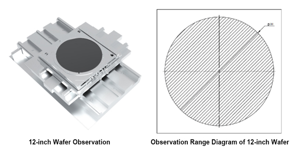
Equipped with an ultra-large travel stage (X/Y ≥ 300 mm), the system provides complete coverage of 12-inch wafers, eliminating the need for sample cutting or transfer. This ensures true "original size, original position" observation. With a Schottky field emission electron gun, it achieves a resolution of 1.0 nm at 15 kV and 1.5 nm at 1 kV, minimizing electron beam damage, making it ideal for sensitive materials and structures.
Key features include:
-
Ultra-large travel stage (X/Y > 300 mm) for full-wafer inspection
-
High-resolution imaging: 1.0 nm at 15 kV and 1.5 nm at 1 kV
-
Automated loading and optical navigation system for fast wafer exchange and precise positioning
-
Intelligent software for auto-focus, astigmatism correction, and multi-format image output
CIQTEK's 12-inch wafer inspection SEM is more than just an observation tool; it's a critical instrument driving higher yields and smaller nodes in semiconductor manufacturing.
September 26–30, Wuhan
CIQTEK will unveil eight cutting-edge electron microscopy solutions at the 2025 Chinese National Conference on Electron Microscopy!
